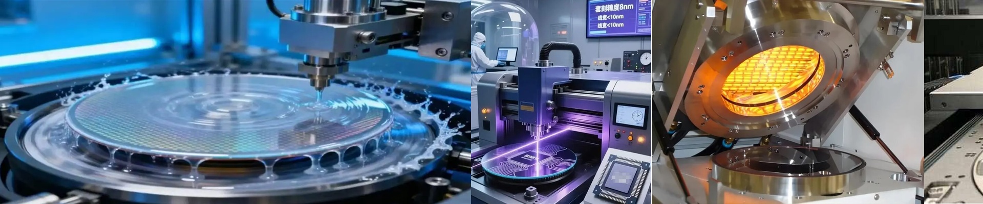

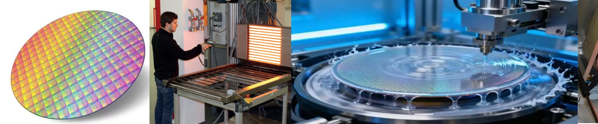
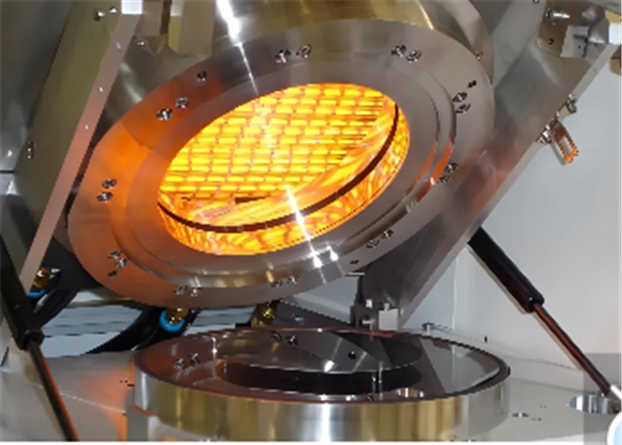
On the fab floor, photoresist bake isn’t optional—it’s a hard constraint. A 2°C drift in soft bake or hard bake will throw off critical dimension control and bleed yield. The heater housing has to turn thermal intent into real performance in the field, without adding particle risk or dragging in thermal inertia.
What actually matters under the hood
We build the stainless steel heater housing around short-wave infrared elements that give you sub-millimeter uniform heat distribution, and it’s repeatable lot after lot. The thermal field tracks setpoint with a tight margin, so your photoresist bake profiles stay in spec. The housing is cleanroom-ready, with welded seams and smooth surfaces that keep particle generation in check. In practice, that translates to fewer lithography excursions and more stable critical dimension uniformity across the wafer.
Why this holds up in a production fab
This housing was built for the floor. It runs 24/7, takes repeated wet cleans, and keeps thermal behavior consistent shift after shift. Wafer-level thermal uniformity stays tight, so you aren’t wasting thermal budget chasing edge-bead artifacts or overcompensating for hot spots. Energy use drops because the response is immediate and the control loop stays quiet. You end up with uptime and repeatability—no marketing spin, just performance you can count on.
What you need to plan for
Think through footprint and service access up front. The stainless housing is compatible with Class 1–100 cleanroom environments, but in high-EMI fab zones, proper grounding and shielding are non-negotiable. Installation is straightforward on standard tool platforms, but alignment and thermal coupling to the process chamber have to be verified during qualification. When those details are nailed, the performance is predictable.